Threshold Crossing Error with Linear Interpolation

21 Feb 2010

Set the sample rate

The upper limit of the frequency response of a digital system is generally less than half of the sample rate.

And from http://en.wikipedia.org/wiki/Rise_time, the rise minimum rise time (10% to 90%) in this system is:

For a test signal, set a rise time and repetition rate

Irrational value helps prevent a fixed ratio of repetition rate to sample rate.

Define the waveform function with a Guassian step (error function)

Normalize σ because the waveform function works on fractions of a period and not abosulte times.

Check the rise time (from 10% to 90%)

Compute a set of zero crossings based on various set of sample points.

Slew Rate at Switching Threshold

Slew rate has an affect on the measurement of jitter as well as the impact of noise on the actual jitter.

To find the peak slew rates which occuring at the switching threshold, scan through the calculated values shown on the Signal Slew Rate plot.

Model of the ADC for Signal Conversion

Set the sample rate. A 4 Gigasample/second scope is good for a 100MHz signal.

And model the size of memory buffer used for the signal capture.

Include the effective number of bits for full scale.

Number of bits for full scale

And define the full scale range. The signal uses nearly the full range.

volts per step

The function to convert the analog (double precision floating point) to a quantized integer value (also stored as double floating point in Mathcad):

A DAC conversion function used to check the operation of the ADC function.

Create a Sample Set

Create a set of samples of the test signal. This test set represents what would be captured in the buffer of a digital oscilloscope.

First column is sample time, and the second is sampled value.

Simulate the quantization effect of ADC

Extract Jitter Information

Global functions (at the end of the sheet) compute a set switching threshold crossing times is computed. This function does a linear interpolation between the quantized points.


The figure below illustrates timing errors that occur with the digitization process.

A worst case timing error can be estimated with geometry. The sample points of the signal about the switching threshold are rounded to the nearest digital value. If both are rounded up or down to the maximum half quantization bin, the the threshold crossing is shifted.

If the threshold level is 0, the width of the crossing error timing is

x1-x2 is the sample period and n depends on the slew rate and the number of ADC bits. Note that maximizing the gain of the oscilloscope amplifier such that either sample point is saturated maximizes the slew rate, but the effective number of bits is 1 because the ADC is functioning as a comparator. At one time, a scope manufacturer recommended this setting for the best accuracy. This may have made sense if there were other amplifier and ADC charactersitics not included here.

In the example here:

ADC counts/sample period

Create a set of threshold crossing times:

Number of clock edges found

Let's compare the interpolated threshold crossing times with the expected times.

Compare the interpolation error to the position of the sample points relative to the threshold crossing.

The following array is a list of the times of the

Create a set of consecutive cycle periods:

Find the time interval between each rising edge.

Check the average of all periods:

time in nanoseconds

error due to quantization

Calculate average period using first and last times:

error due to quantization

Compute Jitter Values Due only to Quantization

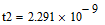
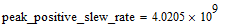
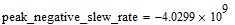
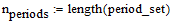
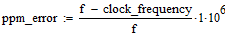
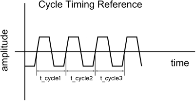
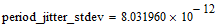
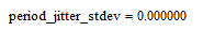
At first cycle jitter seems easy to compute. Just subtract the average period from each cycle period. But from Cypress Semiconductor application note AN5054, "Understanding Data Sheet Jitter Specifications for Cypress Timing Products":


In accordance with JEDEC standard JESD65B, period jitter

is defined as the deviation in cycle time of a signal with

respect to the average period over a random sample of

cycles.


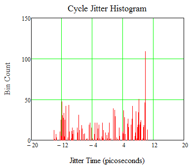
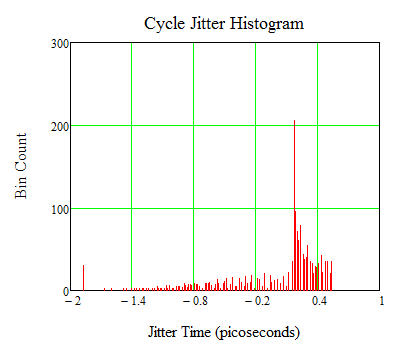
Note the random sample of cycles. If all consecutive cycles are used, some of the error in one cycle would show up as an opposite error in the next cycle. While peak jitter values would not be affected, distributions would be. This is demonstrated later on.


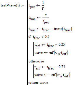
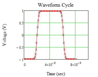
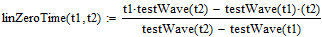
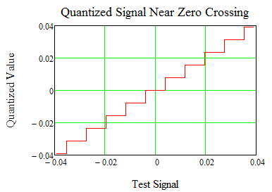
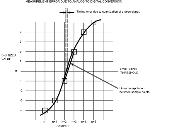
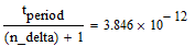
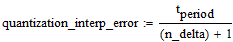
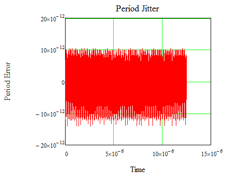
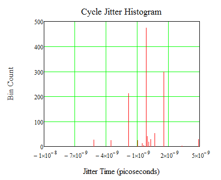
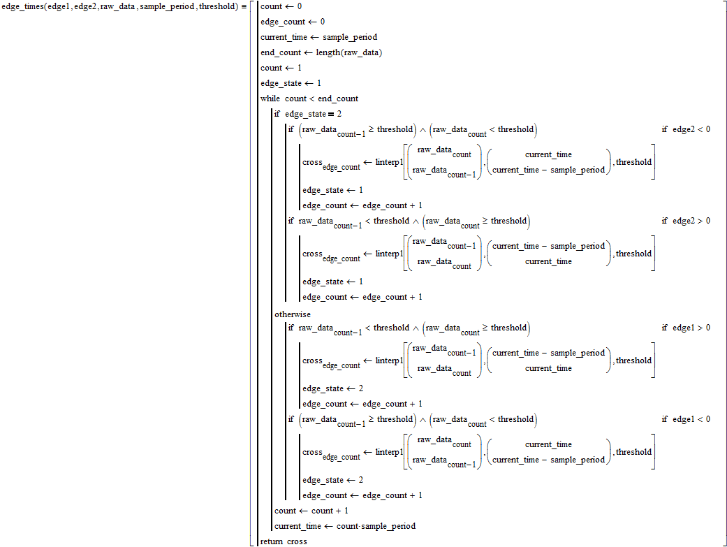
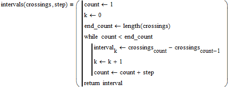
At this point, only quantization error are being considered. With reference to the above figure,


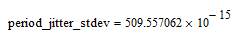
period_jitter=(t_cycle[n]-cycle_average) for n=1,3,5,...


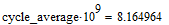
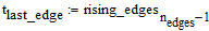
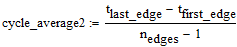
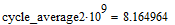
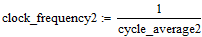
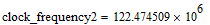
As well, the cycle average used in these calculations will be the computed value from the digitized data.

find the cycle jitter for every second cycle

Form a Histogram

Summary

The simulated peak to peak period jitter is

Estimated peak to peak based on linear interpolation error and quantization error is

The distribution of error is assymetrical because the waveform period is not a multiple of the sample period. As a result, when the first edge of a period has a peak negative error, the positive error on the second edge does not line up with the peak positive error.

Examples with other Clock Frequencies

When measuring period jitter with linear interpolation, the relationship between the signal frequency and the sample clock has a significant impact on the minimum jitter that can be measured. All examples are with a 4GHz sample clock.

Example 1 - 100 MHz Clock 500ps Rise Time

This exmple shows the case where the constant phase relationship between the signal clock and the sample clock produce nearly perfect results. Note, however, a slightly different phase relationship could result in a worse standard deviation.

Example 2 - 101 MHz Clock 500ps Rise Time

Example 3 - 133 MHz Clock 500ps Rise Time

Function to convert absolute time array into time period array:

Function to convert absolute time array into time error array (cumulative jitter)...